The semiconductor industry is changing rapidly, with one of the biggest developments being the move from traditional pogo-based die probing to photonic beam probing for Very-Large-Scale Integration (VLSI) chips. This shift is all about making semiconductor testing more efficient, accurate, and capable of handling the demands of modern technology. Sriharsha Vinjamury, who has worked in this field for 12 years, is a key player in driving this change by developing new methods and techniques.
Why Photonic Beam Probing Is Important for Today's Chip Testing
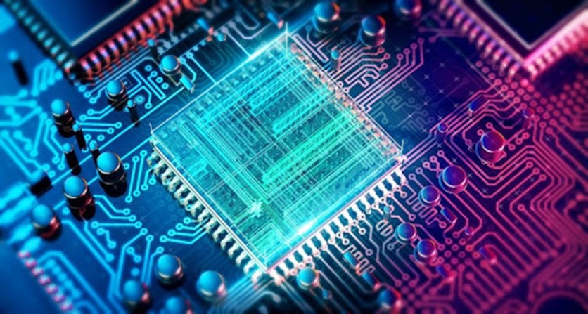
For a long time, the semiconductor industry relied on pogo-based probing, which involves physically touching the chips to test them. However, as chips have become smaller and more complex, this method has run into problems. "As Moore's law advances, the traditional method of wafer probing will see a bottleneck," says Sriharsha Vinjamury. "The physical contact required can actually damage the delicate Wafer bumps, and with the denser layouts of modern chips, it's getting harder to make reliable probe contacts."
Because of these challenges, the industry is looking for better ways to test chips. That's where photonic beam probing comes in. This method uses light instead of physical contact to test silicon wafers. Vinjamury explains, "Photonic beam probing is a big step forward because it saves wafer costs, improves Die yields, and speeds up the testing process."
One of the major advantages of this methodology of probing is its ability to test chips at very high resolutions. "Unlike the status-quo pogo-based contact method, Photonic beam probing doesn't require physical contact, which helps in achieving the Bandwidth for IOs, eliminates probe-tip burns, and saves cost," notes Vinjamury. This is crucial for the semiconductor manufacturing flow because HW-driven defectivity can stop production testing and have adverse downstream effects.
How Sriharsha Vinjamury Is Leading the Way in Semiconductor Post-Silicon Engineering
Sriharsha Vinjamury has been pivotal in advancing post-silicon testing methodologies within the semiconductor industry. During his tenure at Qualcomm, he developed innovative test frameworks that enabled the salvage of partially functional chips—devices that would have otherwise been discarded. This groundbreaking technology quickly gained widespread adoption across the industry. "I'm proud that my work has had a lasting impact, helping to improve yields and reduce waste," Vinjamury reflects.
At Tesla, Vinjamury pushed the boundaries of traditional testing approaches by working on highly complex devices with over 20,000 contact points and more than 100 billion transistors. These cutting-edge chips required exploring new research areas, including the Prototype of photonic probing techniques to test and validate silicon functionality optimally.
As a thought leader and technical manager, Vinjamury has also made significant contributions to addressing the national shortage of semiconductor talent. His efforts have been instrumental in revitalizing local talent pools, supporting the broader vision of bolstering semiconductor manufacturing within the United States. Additionally, he has been deeply involved in establishing state-of-the-art semiconductor testing labs, overseeing budgets in the millions of dollars to create facilities vital for current and future technological advancements.
Vinjamury's impressive achievements and contributions earned him the prestigious role of Principal Engineer at ARM, a position typically reserved for the most senior and experienced engineers. His ability to stay ahead of the curve by at least five years demonstrates his exceptional expertise and forward-thinking approach in the ever-evolving field of semiconductor technology.
Overcoming Challenges and Shaping the Future of Semiconductor Testing
While photonic beam probing offers many benefits, it's not without its challenges. "The initial investment in this technology can be pretty high because of revamping of existing tooling," Vinjamury admits. "And there's a learning curve; we really do not know the Signal and power integrity issues that arise with this approach, and the scalability of the solutions into multiple chip types like." Precision alignment and managing the heat generated by the laser are other hurdles the industry must overcome.
Looking ahead, Vinjamury emphasizes the importance of adopting these new testing methods early on. "There's a real need to explore photonic beam probing, especially as we and others in the semiconductor industry aim to develop chips with 1nm process nodes and the BGA ball pitch going under 10um." Using photonic beams as an alternative to traditional methods could pay off big in the long run.
Despite the challenges, Vinjamury remains committed to refining test methods and embracing new technologies to stay ahead in semiconductor testing. "We're at the cutting edge of chip testing," he says. "By working together—with technology developers, chip manufacturers, or research institutions—we can tackle these challenges and fully realize the benefits of advanced testing methodologies such as this."
Reflecting on his career, Vinjamury adds, "Improvement is a continuous process. As we shift to photonic beams for wafer probing, we're laying the groundwork for a new phase in semiconductor testing. It's a journey of learning and adapting, and I'm glad to be part of it." He's dedicated to encouraging continuous learning within the industry. He believes that by embracing change and staying open to new ideas, the semiconductor industry can keep leading in technological advancements, setting a standard for others to follow.
ⓒ 2026 TECHTIMES.com All rights reserved. Do not reproduce without permission.


